
SPI mode bugs are common because mode numbers are easy to memorize and easy to forget. Timing diagrams are more reliable.
Instead of starting with "mode 0" or "mode 3", start with three questions.
Those questions are:
- What level is the clock when nothing is happening?
- Which clock edge samples the data?
- Does chip select stay active for the whole command?
If you answer those from the datasheet timing diagram, the mode number almost falls out by itself.
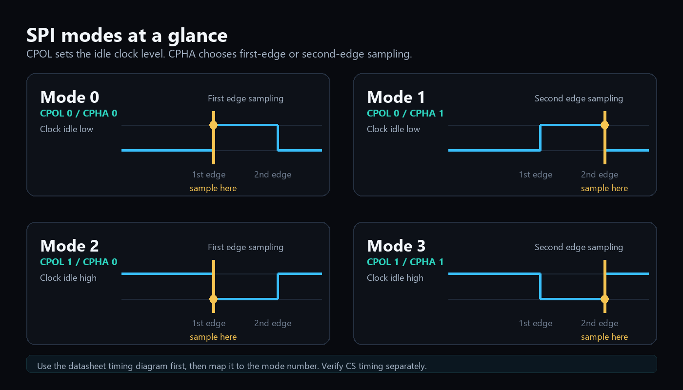
Question 1: What is the idle clock level?
CPOL describes the clock level when the bus is idle.
| CPOL | Idle clock |
|---|---|
| 0 | Low |
| 1 | High |
Look at the datasheet diagram before the first clock pulse. If SCLK rests low, CPOL is 0. If it rests high, CPOL is 1.
This is the easiest part to verify on a logic analyzer. Stop the bus between transactions and look at SCLK. Do not look only at the decoder setting. Look at the waveform.
Question 2: Which edge samples data?
CPHA describes whether data is sampled on the first or second clock edge after chip select becomes active.
| CPHA | Sampling edge |
|---|---|
| 0 | First edge |
| 1 | Second edge |
This is where words like rising and falling can mislead you. The "first edge" depends on CPOL.
If CPOL is 0, the first edge is rising. If CPOL is 1, the first edge is falling.
Think in terms of edges after chip select goes active:
| CPOL | First edge | Second edge |
|---|---|---|
| 0 | Rising | Falling |
| 1 | Falling | Rising |
CPHA tells you which of those two edges is used for sampling.
Question 3: When is data allowed to change?
Data should be stable before the sampling edge and can usually change on the opposite edge. If your capture shows data changing at the same moment the receiver samples it, you are probably in the wrong SPI mode or clocking too fast.
Datasheets usually express this with setup and hold timing:
- Setup time: data must be stable before the sampling edge.
- Hold time: data must remain stable after the sampling edge.
- Propagation delay: how long the slave needs before MISO becomes valid.
This is why a transaction can work at 100 kHz and fail at 8 MHz. The mode may be correct, but the timing margin may be gone.
The four modes
| SPI mode | CPOL | CPHA | Clock idle | Sample edge |
|---|---|---|---|---|
| 0 | 0 | 0 | Low | Rising |
| 1 | 0 | 1 | Low | Falling |
| 2 | 1 | 0 | High | Falling |
| 3 | 1 | 1 | High | Rising |
This table is useful, but the datasheet timing diagram is the source of truth.
A practical way to identify the mode
When a datasheet gives you only a waveform, use this flow:
- Find the inactive clock level before CS goes low.
- Mark that as CPOL.
- Find where the datasheet says data is captured, latched, sampled, or valid.
- Decide whether that is the first or second edge after CS becomes active.
- Mark that as CPHA.
- Convert CPOL and CPHA to the mode number only at the end.
This avoids the common mistake of guessing the mode from a forum post or driver example for a different chip revision.
Mode names are not always written clearly
Some datasheets say "SPI mode 0" directly. Others say things like:
- "Data is captured on the rising edge of SCLK."
- "Data changes on the falling edge."
- "SCLK idles high."
- "The first bit is available before the first clock edge."
- "Sample on the second clock transition."
All of those are timing clues. Read them together. One sentence alone may not be enough.
Field note: when the datasheet is not clear enough
I have run into parts where the datasheet did not make the SPI mode obvious. The timing diagram was there, but the wording around the sampling edge was vague enough that I did not want to trust my first interpretation.
In that situation, I like to make the board tell me the answer during bring-up. At the very beginning of the driver, before any real configuration, I try the same simple register read in all four SPI modes. Usually that means reading a known ID register, such as WHO_AM_I, product ID, device ID, or revision ID.
If one mode returns the expected value and the others return 0x00, 0xFF, or unstable bytes, I have a strong practical signal about which mode the device actually accepts.
This is not something I would leave as normal production behavior forever. It is a bring-up tool. Once the correct mode is known, I hard-code it and keep the probing function around only as a debug helper.
Here is a compact Zephyr-style version of that idea. The example assumes an 8-bit register address, a read bit in bit 7, and one returned byte. Adapt those details to the specific datasheet.
#include <zephyr/device.h>
#include <zephyr/drivers/spi.h>
#include <zephyr/kernel.h>
#include <zephyr/logging/log.h>

LOG_MODULE_REGISTER(spi_probe, LOG_LEVEL_INF);

#define READ_BIT BIT(7)

static int read_reg_u8(const struct device *spi_dev,
                       const struct spi_cs_control *cs,
                       uint16_t operation,
                       uint8_t reg,
                       uint8_t *value)
{
    uint8_t tx_buf[2] = { reg | READ_BIT, 0x00 };
    uint8_t rx_buf[2] = { 0 };

    const struct spi_buf tx = {
        .buf = tx_buf,
        .len = sizeof(tx_buf),
    };
    const struct spi_buf rx = {
        .buf = rx_buf,
        .len = sizeof(rx_buf),
    };

    const struct spi_buf_set tx_set = {
        .buffers = &tx,
        .count = 1,
    };
    const struct spi_buf_set rx_set = {
        .buffers = &rx,
        .count = 1,
    };

    struct spi_config cfg = {
        .frequency = 1000000,
        .operation = operation | SPI_WORD_SET(8) | SPI_TRANSFER_MSB,
        .slave = 0,
        .cs = cs,
    };

    int err = spi_transceive(spi_dev, &cfg, &tx_set, &rx_set);
    if (err) {
        return err;
    }

    *value = rx_buf[1];
    return 0;
}

static int probe_spi_modes(const struct device *spi_dev,
                           const struct spi_cs_control *cs,
                           uint8_t id_reg,
                           uint8_t expected_id)
{
    const uint16_t modes[] = {
        0,
        SPI_MODE_CPHA,
        SPI_MODE_CPOL,
        SPI_MODE_CPOL | SPI_MODE_CPHA,
    };

    for (size_t i = 0; i < ARRAY_SIZE(modes); i++) {
        uint8_t id = 0;
        int err = read_reg_u8(spi_dev, cs, modes[i], id_reg, &id);

        if (err) {
            LOG_WRN("SPI mode %u failed: %d", i, err);
            continue;
        }

        LOG_INF("SPI mode %u read ID 0x%02x", i, id);

        if (id == expected_id) {
            LOG_INF("SPI mode %u looks correct", i);
            return i;
        }
    }

    return -ENODEV;
}
The important part is not the exact code. The important part is the method: choose one register with a known reset value, keep the SPI frequency conservative, keep chip select behavior consistent, and test only one variable at a time.
The logs from that kind of probe should be boring and obvious. Something like this is ideal:
[00:00:01.120] SPI mode 0 read ID 0xff
[00:00:01.124] SPI mode 1 read ID 0x42
[00:00:01.125] SPI mode 1 looks correct
[00:00:01.130] SPI mode 2 read ID 0x00
[00:00:01.134] SPI mode 3 read ID 0x80
That tells me where to look next. If exactly one mode returns the expected ID, I can move forward with confidence. If all four modes return 0xFF, I probably do not have a mode problem; I may have a chip-select, power, reset, MISO, or command-format problem.
When auto-probing can mislead you
Trying all four modes is useful, but it is not magic. A bad test can point you in the wrong direction.
Watch for these traps:
- The SPI clock is too fast, so even the correct mode looks unreliable.
- The read bit is missing from the register address.
- The device requires a dummy byte before valid data.
- Chip select toggles between command and data bytes.
- The ID register is not readable until after a startup delay.
- The device is still in reset or sleep mode.
- The expected ID value depends on the exact part variant.
- A wrong mode accidentally returns a stable-looking byte.
For that reason, I keep the probe simple: low clock speed, one known register, one expected value, and no extra configuration writes before the test.
Why I do not ship this as production auto-detection
SPI mode probing is a bring-up helper, not a long-term driver feature.
I avoid leaving it enabled in production because:
- It makes boot behavior less deterministic.
- It can hide a wrong board or driver configuration.
- It adds unnecessary startup time.
- Some devices may not like invalid transactions immediately after reset.
- It makes failures harder to reason about later.
Once the correct mode is known, I put the mode into the device configuration and keep the probe only behind a debug flag or in a temporary bring-up branch.
Chip select timing matters too
Many SPI failures are blamed on CPOL and CPHA when the real issue is chip select.
Check these values:
- CS setup time before the first clock.
- CS hold time after the last clock.
- Minimum CS high time between transactions.
- Whether multi-byte transfers must keep CS low.
Some devices reset their internal command parser when CS rises. Others expect CS to stay low for command plus address plus data. If firmware toggles CS between bytes, the device may never see a complete command.
For register reads, the transaction often looks like this:
- Pull CS low.
- Send command or register address.
- Send one dummy byte.
- Read returned data on MISO.
- Pull CS high.
If your SPI driver automatically toggles CS after each byte, the device may interpret every byte as a separate command. The waveform will look active, but the response will be wrong.
The first bit problem
CPHA also affects when the first data bit must be ready.
With CPHA = 0, the first data bit is sampled on the first clock edge. That means the transmitter must place that bit on the line before the first edge arrives.
With CPHA = 1, the first edge gives the transmitter time to shift out the first bit, and sampling happens on the second edge.
This is one reason CPHA = 0 captures can look visually surprising: valid data may appear before the first clock pulse.
MSB-first and LSB-first are separate
SPI mode does not define bit order. Most devices use MSB-first, but not all interfaces do, and some controllers can be configured either way.
If the expected ID register is 0x42 but you read 0x24, suspect bit order. If you read a stable but completely different value, also check whether the address needs a read bit or auto-increment bit.
Logic analyzer checklist
When using a logic analyzer, verify the physical waveform before trusting the decoder.
- Confirm SCLK idle level.
- Confirm chip select polarity.
- Look at the first data bit relative to the first edge.
- Compare decoded bytes with raw MOSI/MISO transitions.
- Lower the SPI clock and test again.
If lowering the clock fixes the problem, the mode may be correct but the timing margin is not.
Also check:
- Does CS stay low across the whole command?
- Does the register address include the required read bit?
- Is the first MISO byte dummy data?
- Is the expected response MSB-first?
- Are voltage levels valid for both devices?
What to ask a datasheet AI
Good SPI questions are narrow and easy to cite:
- "Which SPI mode does this datasheet require?"
- "Does SCLK idle high or low?"
- "On which clock edge is MOSI sampled?"
- "What is the maximum SPI clock frequency?"
- "Does chip select need to stay low for multi-byte reads?"
- "Is a dummy byte required before valid read data?"
Then inspect the cited page and compare it with your analyzer capture.
A small debug example
Imagine a sensor has a WHO_AM_I register at 0x0F and the expected value is 0xD1. Your firmware reads 0xFF.
Work down the stack:
- Is the sensor powered and out of reset?
- Is CS going low on the correct pin?
- Is SCLK idle at the datasheet's required level?
- Is data sampled on the required edge?
- Did you set the read bit in the address byte?
- Does the part require a dummy byte before the answer?
- Is MISO physically connected and at the correct voltage?
If every read is 0xFF, the slave may not be driving MISO at all. If reads are stable but wrong, the mode, command format, or bit order may be wrong.
Takeaway
SPI mode is not magic. It is just idle clock level plus sample edge. Read those from the timing diagram, then verify chip select timing and bus speed before changing firmware blindly.